The Role of Cryogenics in Semiconductor Manufacturing
A Deep Dive into Ultra-Cold Precision
The semiconductor industry drives technological innovation, powering everything from smartphones to spacecraft. As semiconductor devices become increasingly complex and miniaturized, the demand for precise manufacturing environments continues to rise. Cryogenics, the science of ultra-low temperatures, plays a pivotal role in meeting these demands by offering unparalleled control, efficiency, and quality during semiconductor fabrication.
In this detailed exploration, we’ll uncover how cryogenic technologies are revolutionizing semiconductor manufacturing, enhancing product quality, reducing defects, and enabling the next generation of microelectronics.
Understanding Cryogenics in Semiconductor Production
What Is Cryogenics?
Cryogenics refers to the production and behavior of materials at extremely low temperatures, typically below −180°C (−292°F). Key cryogenic fluids used in the semiconductor industry include:
- Liquid nitrogen (LN2)
- Liquid helium (LHe)
- Liquid argon (LAr)
These cryogens help control thermal processes critical to semiconductor manufacturing.
Why Cryogenics Matter in Microelectronics
Cryogenics enable:
- Precise thermal control during fabrication
- Contamination reduction by freezing out impurities
- Enhanced vacuum performance for deposition and etching
- Material stress testing under extreme conditions
Key Applications of Cryogenics in Semiconductor Manufacturing
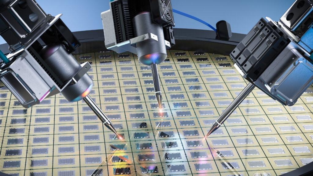
Cryogenic Cooling for Wafer Processing
Modern wafer fabrication requires exact temperature management.
Benefits of Cryogenic Cooling:
- Minimizes thermal expansion to maintain structural integrity
- Reduces particle contamination by freezing airborne particulates
- Improves etching and deposition uniformity
Cooling Techniques:
- Helium-cooled electrostatic chucks (ESCs) for holding wafers
- Cryogenic vapor delivery in chemical vapor deposition (CVD) and etching systems
Vacuum Systems and Cryopumping
Vacuum environments are essential for many semiconductor processes.
Cryopumping Advantages:
- Superior vacuum levels through gas condensation
- Lower operational noise compared to mechanical pumps
- Reduced risk of oil contamination
Applications:
- Molecular beam epitaxy (MBE)
- Physical vapor deposition (PVD)
- Ion implantation
Extreme Ultraviolet Lithography (EUV)
EUV lithography, critical for next-gen chips, demands sophisticated cryogenic systems.
Cryogenic Roles in EUV:
- Cooling of light sources
- Controlling wafer and mask temperatures
- Suppressing thermal drift during patterning
Cryogenic Testing of Semiconductor Devices
Testing ensures chips function correctly across all environments.
Common Cryogenic Testing Applications:
- Thermal cycling tests for material endurance
- Low-temperature electrical characterization
- Space-grade semiconductor qualification

Challenges in Cryogenic Applications
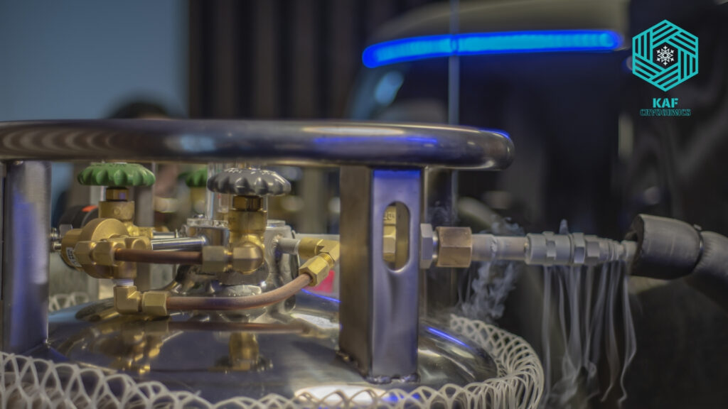
Handling and Storage of Cryogens
Cryogens require careful handling to prevent accidents.
- Double-walled vacuum-insulated tanks
- Pressure relief and venting systems
- Personal protective equipment (PPE) for operators
System Integration Complexities
Integrating cryogenic systems into semiconductor fabs can be complex due to:
- Space constraints
- Energy demands
- Maintenance requirements
Thermal Management
Rapid temperature changes can stress delicate components.
Solutions include:
- Gradual ramping protocols
- Real-time thermal monitoring
- Redundant cooling loops
Innovations Driving the Future
Cryogenic Substrates
Using cryogenically cooled substrates during deposition improves film quality.
- Reduced defects and dislocations
- Enhanced adhesion properties
Green Cryogenics
Focus on sustainability is growing.
- Helium recycling systems to minimize gas loss
- Energy-efficient cryocoolers
- Hybrid vacuum systems combining cryopumping and turbomolecular pumps
Automation and Smart Monitoring
Modern fabs employ IoT-enabled cryogenic systems for predictive maintenance.
- Sensor networks monitoring temperature, pressure, and flow
- AI-driven analytics to detect anomalies
- Remote system diagnostics
Best Practices for Implementing Cryogenics in Semiconductor Facilities
System Design and Planning
- Early integration during fab planning
- Modular designs for easy upgrades
- Redundant systems to ensure uptime
Safety First
- Comprehensive cryogen training for staff
- Emergency shutdown systems
- Oxygen deficiency monitoring in enclosed spaces
Maintenance and Upkeep
- Scheduled cryocooler servicing
- Routine leak detection
- Cryogen inventory management
KAF Cryogenics: Your Partner in Semiconductor Excellence
At KAF Cryogenics, we specialize in engineering advanced cryogenic solutions tailored for the semiconductor industry.
Our Offerings:
- Custom-designed cryogenic cooling systems
- High-performance vacuum insulation technologies
- Integrated cryogenic testing chambers
Why Choose Us?
- Unmatched precision engineering
- Compliance with SEMI and ISO standards
- Proactive customer support
Explore how we can help optimize your semiconductor production with ultra-reliable cryogenic solutions. Contact us today to learn more.
Cooling the Future of Microelectronics
Cryogenic technologies are not just an accessory in semiconductor manufacturing—they are a cornerstone of innovation, reliability, and scalability. As chips become smaller, faster, and more complex, the role of cryogenics will only grow more essential.
KAF Cryogenics remains committed to powering this future with cutting-edge, energy-efficient solutions designed to meet the evolving needs of the semiconductor industry.
Stay tuned with KAF Cryogenics for the latest advancements shaping the future of microelectronics and cryogenic engineering.