Cryogenic Innovations in the Electronics Industry
Pushing Boundaries with Subzero Precision
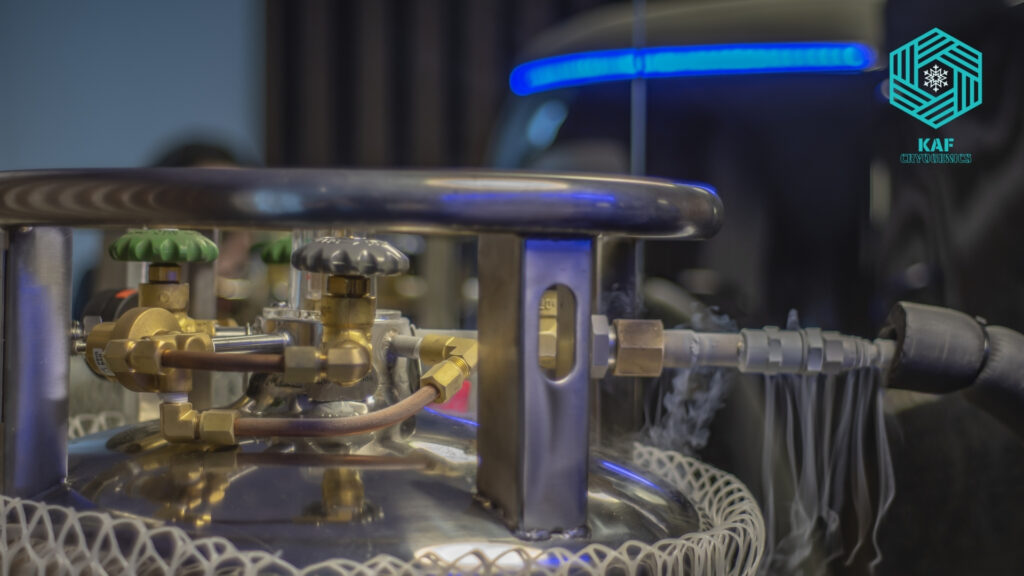
In the ever-evolving world of electronics, where miniaturization and performance go hand in hand, cryogenic technology is emerging as a powerful enabler. By operating at ultra-low temperatures, cryogenic systems can significantly enhance the performance, efficiency, and reliability of electronic devices. From quantum computing and superconductors to semiconductor fabrication and high-performance sensors, cryogenics is playing an increasingly critical role.
In this blog, we explore how cryogenic innovations are transforming the electronics industry, driving scientific discovery and enabling next-generation advancements. Companies like KAF Cryogenics are at the forefront, designing specialized cryogenic equipment tailored to the demanding needs of electronics manufacturers and researchers.
Cryogenics in Quantum Computing
Redefining Computational Power
Quantum computing operates on the principles of quantum mechanics, which require components like qubits to be kept at near-absolute-zero temperatures. Cryogenic systems create these environments, reducing noise and thermal fluctuations that interfere with quantum states.
Key Cryogenic Technologies for Quantum Computers:
- Dilution refrigerators: Provide cooling down to 10 millikelvin
- Cryogenic amplifiers: Improve signal integrity at low noise levels
- Thermal shields and vacuum chambers: Ensure stable cryo-environments
Real-World Applications
- Cryptography and secure communications
- Drug discovery through molecular simulation
- Optimization problems in logistics and AI
Enhancing Superconducting Electronics
Unlocking Zero Resistance
Superconductors are materials that conduct electricity with zero resistance when cooled below a critical temperature. This makes them ideal for high-speed, low-power electronics and powerful magnetic field generation.
Benefits of Cryogenic Superconductors:
- Energy efficiency: No energy loss due to resistance
- Higher processing speeds: Ideal for ultrafast switches and logic circuits
- Miniaturization potential: Enables compact design of complex circuitry
Applications in Modern Electronics
- Digital-to-analog converters in signal processing
- RF filters in mobile communications
- Superconducting qubits in quantum computing
Semiconductor Fabrication at Cryogenic Temperatures
Precision in Nano-Scale Engineering
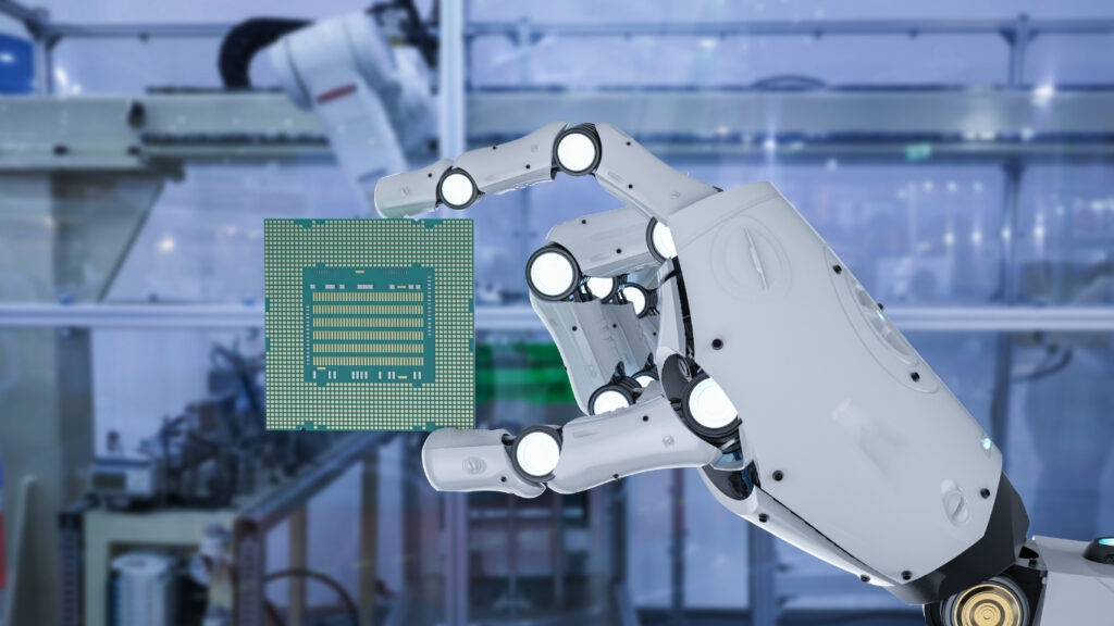
In semiconductor manufacturing, cryogenics plays a role in improving lithography accuracy, enhancing etching precision, and controlling contamination during wafer processing.
Cryogenic Integration in Fabrication:
- Cryo-etching: Uses ultra-cold gases for clean, damage-free patterning
- Cryo-pumping: Achieves ultra-high vacuum conditions for deposition
- Cryo-CMP (chemical-mechanical polishing): Enhances surface smoothness
Benefits for Chip Manufacturers
- Improved yield and uniformity
- Reduced defect density
- Scalability to sub-5nm process nodes
Cryogenic Cooling for High-Performance Sensors
Enabling Extreme Sensitivity
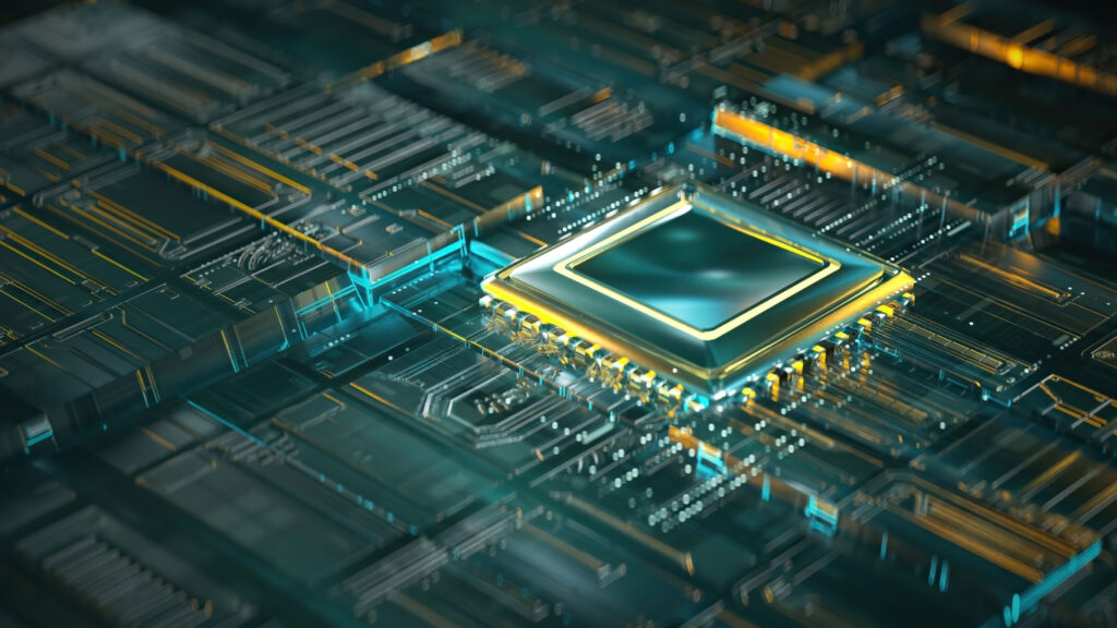
Many electronic sensors—especially those used in space, defense, and scientific instruments—perform best at cryogenic temperatures. Cooling reduces thermal noise, allowing for more accurate measurements.
Types of Sensors Benefiting from Cryogenics:
- Infrared detectors: For thermal imaging and astronomy
- X-ray and gamma-ray detectors: For space telescopes and medical diagnostics
- Magnetometers: Used in geological surveys and particle physics
Integration and Use Cases
- Night-vision systems
- Satellite imaging payloads
- Lab-grade scientific instruments
Cryogenic Testing and Validation
Stress Testing Under Extreme Conditions
Electronic components destined for harsh environments—like space or high-radiation zones—must be tested at cryogenic temperatures. This ensures reliability under operational extremes.
Cryogenic Testing Advantages:
- Simulates real-world thermal stress
- Identifies material behavior at low temperatures
- Ensures product integrity for mission-critical systems
Commonly Tested Devices
- Microprocessors and ASICs
- MEMS components
- PCB materials and interconnects
KAF Cryogenics: Supporting Innovation in Electronics
Engineering Solutions for the Electronics Sector
KAF Cryogenics collaborates with electronics companies and research labs to design and deliver high-performance cryogenic systems. From lab-scale cooling setups to industrial-grade solutions, KAF offers:
Our Key Solutions Include:
- Custom cryostats and chambers
- Low-loss cryogenic transfer lines
- Helium and nitrogen re-condensation systems
- High-vacuum insulation technologies
Designed for Compliance and Innovation
All KAF Cryogenics equipment is engineered to meet the rigorous standards of the electronics sector:
- ISO 14644 for cleanroom compatibility
- SEMI standards for semiconductor tools
- RoHS and CE certifications for electronic compliance
Looking Ahead: Cryogenics and the Future of Electronics
As the demand for performance, efficiency, and miniaturization continues to rise, cryogenic technology will remain a vital part of the electronics landscape. Whether enabling the quantum revolution or refining nano-manufacturing processes, cryogenics is shaping the future of electronic innovation.
Ready to integrate cryogenics into your electronics project? Contact KAF Cryogenics today to explore our customized cryogenic solutions for the electronics industry.